


Please Leave Us A Message
Privacy statement: Your privacy is very important to Us. Our company promises not to disclose your personal information to any external company with out your explicit permission.

Shenzhen Yetai Optoelectronics Technology Co.,Ltd.
Model No.: 100002N0-1000
Payment Type: T/T
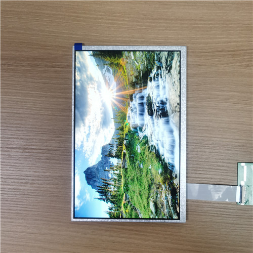
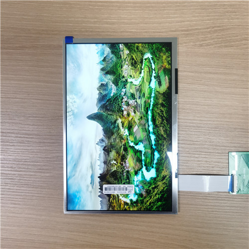
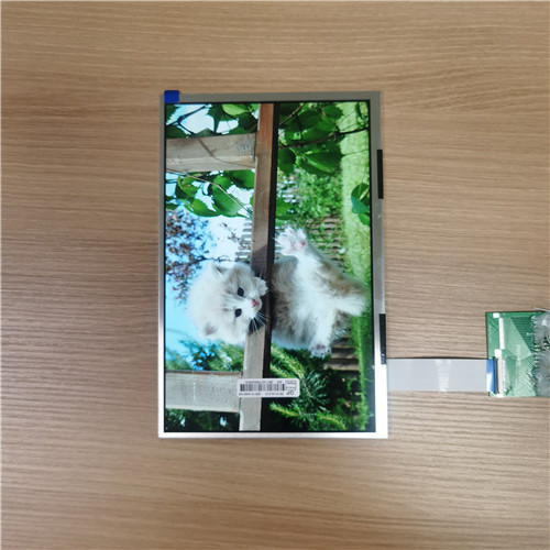
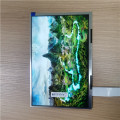
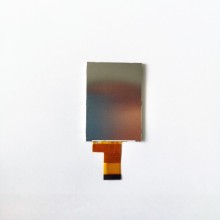
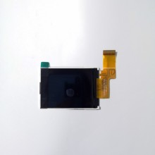
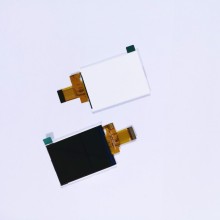
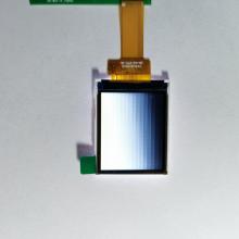
10.1 Inch Lcd Tft Display
An LCD consists of many pixels. A pixel consists of three sub-pixels (Red/Green/Blue, RGB). In the case of Full-HD resolution, which is widely used for smartphones, there are more than six million (1,080 x 1,920 x 3 = 6,220,800) sub-pixels. To activate these millions of sub-pixels a TFT is required in each sub-pixel. TFT is an abbreviation for "Thin Film Transistor". A TFT is a kind of semiconductor device. It serves as a control valve to provide an appropriate voltage onto liquid crystals for individual sub-pixels. A TFT LCD has a liquid crystal layer between a glass substrate formed with TFTs and transparent pixel electrodes and another glass substrate with a color filter (RGB) and transparent counter electrodes. In addition, polarizers are placed on the outer side of each glass substrate and a backlight source on the back side. A change in voltage applied to liquid crystals changes the transmittance of the panel including the two polarizing plates, and thus changes the quantity of light that passes from the backlight to the front surface of the display. This principle allows the TFT LCD to produce full-color images.


| No. | Item | Specification | Remark |
| 1 | LCD size | 10.1 inch(Diagonal) |
|
| 2 | Driver element | a-Si TFT active matrix |
|
| 3 | Resolution | 1280 × 3(RGB) × 800 |
|
| 4 | Display mode | Normally Black, Transmissive |
|
| 5 | Dot pitch | 0.0565(W) × 0.1695(H) mm |
|
| 6 | Active area | 216.96(W) × 135.60(H) mm |
|
| 7 | Module size | 229.46(W) ×149.1(H) ×2.5(D) mm | Note 1 |
| 8 | Surface treatment | Hard Coating (3H) |
|
| 9 | Color arrangement | RGB-stripe |
|
| 10 | Interface | LVDS |
|
| 11 | Backlight power consumption | TBD |
|
| 12 | Panel power consumption | (1W)(Typ.) | Note 2 |
| 13 | Weight | TBD(Typ.) |
|
Note 1: Refer to Mechanical Drawing.
Note 2: Including T-con Board power consumption
A 40pin connector is used for the module electronics interface. The recommended model is F62240-H1210A manufactured by Vigorconn.
| Pin No. | Symbol | I/O | Function | Remark |
| 1 | VCOM | P | Common Voltage |
|
| 2 | VDD | P | Power Supply |
|
| 3 | VDD | P | Power Supply |
|
| 4 | NC | --- | No connection |
|
| 5 | NC | --- | No connection |
|
| 6 | NC | --- | No connection |
|
| 7 | GND | P | Ground |
|
| 8 | Rxin0- | I | -LVDS Differential Data Input |
R0-R5, G0 |
| 9 | Rxin0+ | I | +LVDS Differential Data Input | |
| 10 | GND | P | Ground |
|
| 11 | Rxin1- | I | -LVDS Differential Data Input |
G1~G5, B0,B1 |
| 12 | Rxin1+ | I | +LVDS Differential Data Input | |
| 13 | GND | P | Ground |
|
| 14 | Rxin2- | I | -LVDS Differential Data Input | B2-B5,HS,VS, DE |
| 15 | Rxin2+ | I | +LVDS Differential Data Input | |
| 16 | GND | P | Ground |
|
| 17 | RxCLK- | I | -LVDS Differential Clock Input |
LVDS CLK |
| 18 | RxCLK+ | I | +LVDS Differential Clock Input | |
| 19 | GND | P | Ground |
|
| 20 | Rxin3- | I | -LVDS Differential Data Input | R6, R7, G6, G7, B6, B7 |
| 21 | Rxin3+ | I | +LVDS Differential Data Input | |
| 22 | GND | P | Ground |
|
| 23 | NC | --- | No connection |
|
| 24 | NC | --- | No connection |
|
| 25 | GND | P | Ground |
|
| 26 | NC | --- | No connection |
|
| 27 | LED_PWM | O | CABC controller signal output for backlight | Note2 |
| 28 | NC | --- | No connection |
|
| 29 | AVDD | P | Power for Analog Circuit |
|
| 30 | GND | P | Ground |
|
| 31 | LED- | P | LED Cathode |
|
| 32 | LED- | P | LED Cathode |
|
| 33 | NC | --- | No connection |
|
| 34 | NC | --- | No connection |
|
| 35 | VGL | P | Gate OFF Voltage |
|
| 36 | NC | --- | No connection |
|
| 37 | CABC_EN | I | CABC Enable Input | Note1 |
| 38 | VGH | P | Gate ON Voltage |
|
| 39 | LED+ | P | LED Anode |
|
| 40 | LED+ | P | LED Anode |
|
I: input, O: output, P: Power
Note1: The setting of CABC function are as follows.
| Pin | Enable | Disable |
| CABC_EN | High Voltage | Low Voltage or open |
Note2: LED_PWM is used to adjust backlight brightness.
Luminance Bright
Luminance Dark
Duty (0%) Duty (100%)
(Note 1)
|
Item |
Symbol | Values |
Unit |
Remark | |
| Min. | Max. | ||||
|
Power voltage | VDD | -0.3 | 3.9 | V |
|
| AVDD | -0.3 | 14 | V |
| |
| VGH | -0.3 | 42.0 | V |
| |
| VGL | -19 | 0.3 | V |
| |
| VGH-VGL | 12 | 40.0 | V |
| |
| Operation Temperature | TOP | -10 | 50 | ℃ |
|
| Storage Temperature | TST | -20 | 60 | ℃ |
|
| LED Reverse Voltage | VF | 2.7 | 3.1 | V | IF=20mA |
| LED Forward Current | IR | --- | 50 | mA | VR=5V |
Note 1: The absolute maximum rating values of this product are not allowed to be exceeded at any times. Should a module be used with any of the absolute maximum ratings exceeded, the characteristics of the module may not be recovered, or in an extreme case, the module may be permanently destroyed.
3.1.1. Current Consumption
|
Item |
Symbol | Values |
Unit |
Remark | ||
| Min. | Typ. | Max. | ||||
|
Current for Driver | IGH | - | STB | STB | mA | VGH =22V |
| IGL | - | STB | STB | mA | VGL = -7V | |
| IVDD | - | STB | STB | mA | VDD =2.5V | |
| IAVDD | - | STB | STB | mA | AVDD =8.2V | |
3.1.2. Backlight Driving Conditions
|
Item |
Symbol | Values |
Unit |
Remark | ||
| Min. | Typ. | Max. | ||||
| Voltage for LED backlight | VL | 17.1 | 18.0 | 18.9 | V | Note 1 |
| Current for LED backlight | IL | - | 300 | - | mA |
|
| LED life time | - | 20000 | 25000 | 30000 | Hr | Note 2 |
Note 1: The LED Supply Voltage is defined by the number of LED at Ta=25℃ and IL =300mA.
Note 2: The “LED life time” is defined as the module brightness decrease to 50% original brightness at Ta=25℃ and IL =300mA. The LED lifetime could be decreased if operating IL is lager than 300mA.
( Note 1)
|
Item |
Symbol | Values |
Unit |
Remark | ||
| Min. | Typ. | Max. | ||||
|
Power voltage | VDD | 2.3 | 2.5 | 2.7 | V | Note 2 |
| AVDD | 8.0 | 8.2 | 8.4 | V |
| |
| VGH | 21.7 | 22 | 22.3 | V |
| |
| VGL | -7.3 | -7 | -6.7 | V |
| |
| Input signal voltage | VCOM | 3.0 | 3.3 | 3.6 | V | Note 4 |
| Input logic high voltage | VIH | 0.8 VDD | - | 3.6 | V |
Note 3 |
| Input logic low voltage | VIL | 0 | - | 0.2 DVDD | V | |
Note 1: Be sure to apply VDD and VGL to the LCD first, and then apply VGH.
Note 2: VDD setting should match the signals output voltage (refer to Note 3) of customer’s system board.
Note 4: Typical VCOM is only a reference value, it must be optimized according to each LCM. Be sure to use VR.
a. Power on:
0.5ms< T1<10ms
b. Power off:
VDD
0.5ms< T1<10ms
LVDS
Signal
VGH
VGL
AVDD
VCOM
B/L
3.4.1. AC Electrical Characteristics
| Parameter | Symbol | Values | Unit | Remark | ||
| Min. | Typ. | Max. | ||||
| LVDS Differential input high Threshold voltage | RxVTH | - | - | +100 | mV |
RXVCM=1.2V |
| LVDS Differential input low Threshold voltage | RxVTL | -100 | - | - | mV | |
| LVDS Differential input common mode voltage | RxVCM | 0.7 | - | 1.6 | V |
|
| LVDS Differential voltage | |VID| | 100 | - | 600 | mV |
|
| |
3.4.2. Timing Table
|
Item |
Symbol | Values |
Unit |
Remark | ||
| Min. | Typ. | Max. | ||||
|
Clock Frequency |
1/Tc |
(68.9) |
71.1 |
(73.4) |
MHz | Frame rate =60Hz |
| Horizontal display area | tHD | 1280 | Tc |
| ||
| HS period time | tH | (1410) | 1440 | (1470) | Tc |
|
| HS Width +Back Porch +Front Porch | tHW+ tHBP +tHFP | (60) | 160 | (190) | Tc |
|
| Vertical display area | tVD | 800 | tH |
| ||
| VS period time | tv | (815) | 823 | (833) | tH |
|
| VS Width +Back Porch +Front Porch | tvW+ tvBP +tvFP | (15) | 23 | (33) | tH |
|
| |
3.4.3. LVDS Data Input Format
| |
|
Item |
Symbol |
Condition | Values |
Unit |
Remark | ||
| Min. | Typ. | Max. | |||||
|
Viewing angle (CR≥ 10) | θL | Φ=180°(9 o’clock) | 75 | 85 | - |
degree |
Note 1 |
| θR | Φ=0°(3 o’clock) | 75 | 85 | - | |||
| θT | Φ=90°(12 o’clock) | 75 | 85 | - | |||
| θB | Φ=270°(6 o’clock) | 75 | 85 | - | |||
|
Response time | TON |
Normal θ=Φ=0° | - | 10 | 20 | msec | Note 3 |
| TOFF | - | 15 | 30 | msec | Note 3 | ||
| Contrast ratio | CR | 600 | 800 | - | - | Note 4 | |
|
Color chromaticity | WX | 0.27 | 0.31 | 0.35 | - | Note 2 Note 5 Note 6 | |
| WY | 0.30 | 0.33 | 0.38 | - | |||
| Luminance | L | 900 | 1000 | - | cd/m2 | Note 6 | |
| Luminance uniformity | YU | 75 | 80 | - | % | Note 7 | |
Product Categories : TFT LCD > 10.1 Inch TFT LCD


Privacy statement: Your privacy is very important to Us. Our company promises not to disclose your personal information to any external company with out your explicit permission.
Fill in more information so that we can get in touch with you faster
Privacy statement: Your privacy is very important to Us. Our company promises not to disclose your personal information to any external company with out your explicit permission.